• Ferroic and multiferroic topological structures offer exciting potential in future nanoelectronics
• Commentary piece published this week in Nature Materials
Fig 1. Invited review author Prof Jan Seidel (UNSW)
The connection from fridge magnets to cutting edge materials science is shorter than what one might expect. The reason why a magnet sticks to your fridge is that electronic spins or magnetic moments in the magnetic material spontaneously align or order in one direction, which enables it to exert an attractive force to the steel door of your fridge and reminds you to buy milk.
Magnets are one type of materials with such built-in order. A ‘topological defect’ in such a material occurs as a discontinuity in this order, i.e. a boundary region where the order does not seamlessly transition from one area to another. These topological structures form naturally or can be highly engineered in advanced functional materials.
An article published this week in the leading journal Nature Materials by FLEET CI Prof Jan Seidel outlines emerging research into different types of ‘defective’ order, i.e. topological structures in materials, and their potential highly interesting applications in nanotechnology and nanoelectronics. Seidel was invited by the journal editor to review current and discuss future research on domain walls and related topological structures.
Domain walls
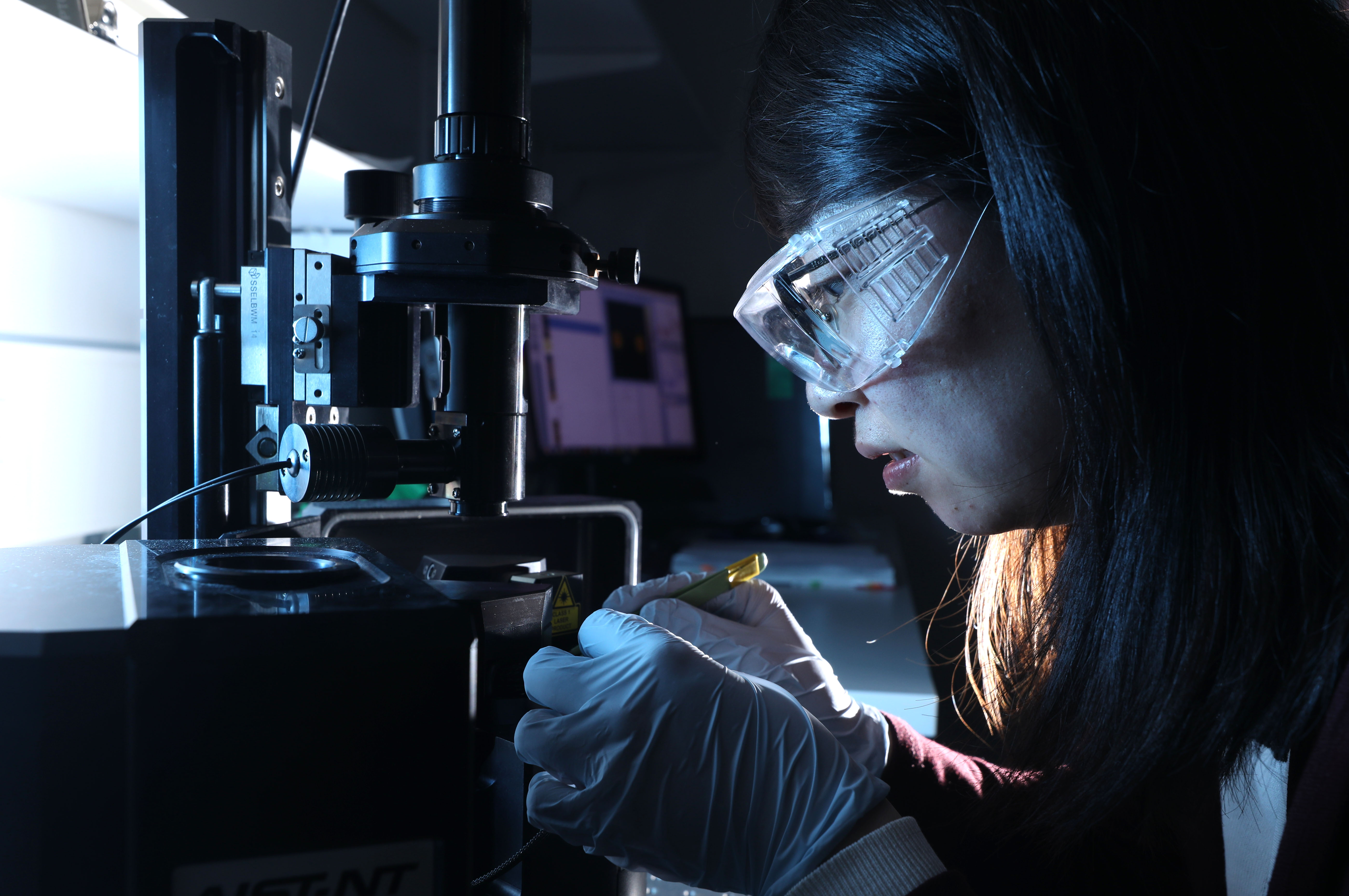
Fig 2. FLEET PhD student Fan Ji in Prof Seidel’s group, using SPM to study materials
Although known for a long time, domain walls as one type of topological structure have only been intensively studied in detail over recent years. It is only with recent developments in high-resolution electron microscopy (HREM) and scanning probe microscopy (SPM) that it has been shown that they can significantly affect macroscopic materials properties, and even more interestingly, that they can exhibit intrinsic properties of their own. Research in this field pioneered in part by Prof Seidel has grown extensively in the last few years and now has entire conferences dedicated to it, such as the annual International Workshop on Topological Structures in Ferroic Materials (TOPO), for which the first meeting was held in 2015 in Sydney.
A substantial amount of recent work on domain walls has focussed on electronic conductivity at such walls in otherwise insulating ferroelectrics and multiferroics, opening new opportunities for nanoelectronics. Such walls are only about 1nm wide (current silicon technology is at 7nm structure sizes), making them the ultimate nanoelectronics feature.
Domain wall nanoelectronics has given rise recently to prototype electronic elements such as diodes, non-volatile memory, and tunnel-junctions, whose functions are driven by external stimuli, such as an applied electric field or applied light. The controlled engineering of topological defects and their manipulation with applied fields, nanoscale probes and devices will enable a wide range of new phenomena to be explored at atomic and nanometre scales.
Vortices and skyrmions
Other more complex topological structures (Fig. 3) such as vortices and skyrmions (exotic topological quasiparticles that are their own antiparticle) can be observed, created and manipulated in ferroic materials, and are the focus of intense research efforts to exploit their structure, symmetry, chemistry and unique properties for nanoelectronics.
Potential applications of topological materials, including dissipationless or ultra-low energy electronic transport technologies, are an emerging field that is being extensively studied (including within FLEET).
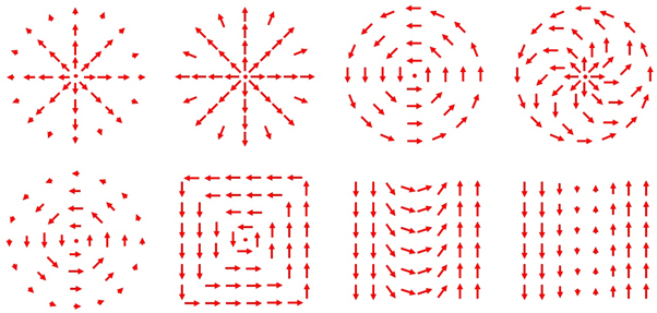
Fig 3. Various types of order and topological defects found in materials.
Topological structures themselves can carry information and be displaced on the nanometre scale, with skyrmions being one prominent example. Magnetic ‘whirl’ structures hosting skyrmions have high potential for future ultra-low energy memory and logic applications.
With a cornucopia of exciting recent developments and progress in these areas, and with many more likely to come, the field of topological electronics has opened a variety of new and interesting prospects in advanced materials research, and has a bright future ahead with potential applications in new device concepts, ultra-low energy nanoelectronics and dissipationless transport technologies.
THE STUDY
Nanoelectronics based on topological structures (DOI 10.1038/s41563-019-0301-z) was published in Nature Materials on 20 February 2019. Prof Seidel acknowledges funding support by the Australian Research Council (ARC) through Discovery Grants and the ARC Centre of Excellence in Future Low Energy Electronics Technologies (FLEET).
TOPOLOGICAL MATERIALS AND FLEET
 Topological materials are investigated within FLEET’s Research theme 1, seeking ultra-low resistance electronic paths with which to create a new generation of ultra-low energy electronics.
FLEET is an ARC-funded research centre bringing together over a hundred Australian and international experts to develop a new generation of ultra-low energy electronics, motivated by the need to reduce the energy consumed by computing.
Prof Seidel performs key scanning probe microscopy (SPM) based research for FLEET’s Research theme 1 and Theme 2, with a particular focus on complex oxide-material systems. Seidel also uses advanced SPM techniques to pattern electrical or magnetic order in topological materials at the nanoscale in Enabling technology theme B.
THE AUTHOR
Prof Jan Seidel is a Professor at the School of Materials Science and Engineering at UNSW Sydney.
MORE INFORMATION
- Contact Prof Jan Seidel UNSW jan.seidel@unsw.edu.au
- Visit Seidel Research Group SPM.materials.unsw.edu.au
- Connect at @FLEETCentre
- Visit FLEET.org.au
- Read FLEET Research theme 1 news
- Contact FLEET media@FLEET.org.au
- Watch Future solutions to computation energy use
- Subscribe FLEET.org.au/news
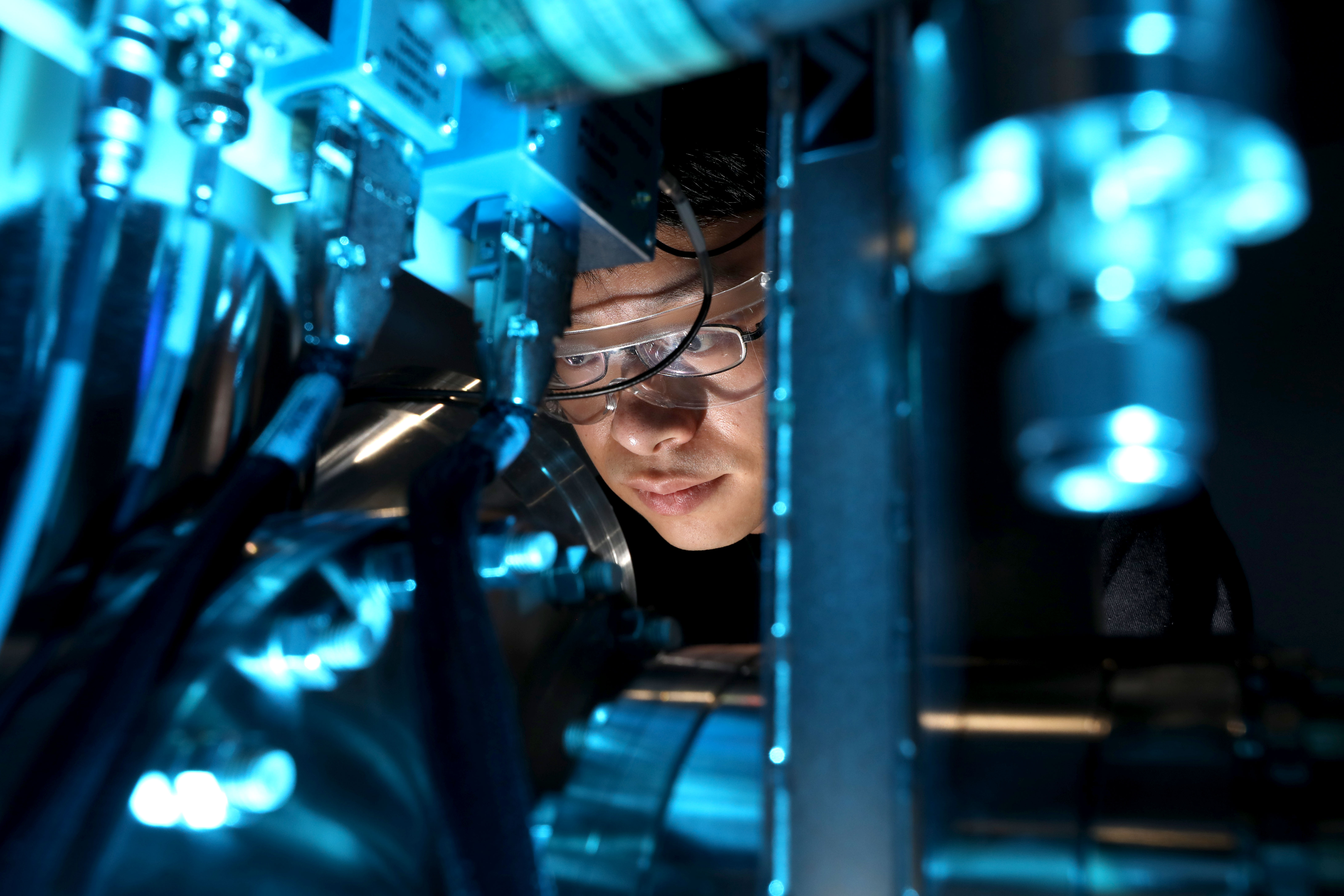
Fig 5. FLEET PhD student Fei Hou in Prof Seidel’s group, using SPM to study materials