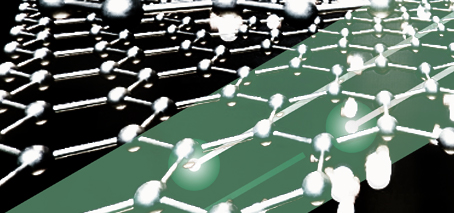
The famous, symmetrical ‘honeycomb’ structure of graphene is the reason for its remarkable electronic properties
- New facility improves study of ‘artificial graphene’ at FLEET
- ‘Like driving a new Maserati!’
The amazing electrical properties of graphene and other 2D, atomically-thin crystals are due to the symmetry of their lattice structure.
For example, it is graphene’s famous ‘honeycomb’ lattice that causes electrons to act as they were massless – moving about 70 times faster than in silicon (the semiconductor material used in most computer processors today).
(Incidentally, this is also the reason why it is so difficult to make graphene transistors. They are always ON, and are difficult to turn OFF.)
Graphene and similar 2D materials face a challenge before they could be used in any commercially-viable future electronics technology: The techniques currently used to fabricate graphene are not robust or scalable enough for industrial manufacturing.
One promising, alternative approach is to ‘engineer’ an artificial version of graphene, using conventional semiconductor materials, to match industrial requirements.
FLEET uses advanced nanofabrication techniques to manipulate the surface structure of such semiconductors, creating the necessary pattern at a nanometre-scale to precisely recreate the electronic structure of graphene and 2D topological insulators.
Working at scales of millionths of a millimetre, such nano-engineered materials are called artificial analogs of graphene and 2D topological insulators, or simply ‘artificial graphene’.

Oleg Klochan and Daisy Wang study artificial graphene at UNSW
“This is not a trivial task,” explains FLEET’s Dr. Oleh Klochan, who leads this research at UNSW.
“The creation of synthetic, defect-free periodic lattices in conventional materials that successfully mimic graphene or topological insulators requires precise and accurate positioning of the lattice sites with a nanometre resolution,” says Dr Klochan.
A new atomic layer deposition system, supported by FLEET funding, has recently been commissioned for this project, and is now fully operational.
“We are using this now to make samples and we are extremely happy with it,” says Oleh. “It’s like you have been driving a very old car for years (and it was breaking down all the time and mechanics couldn’t fix it either) and now you have got a brand new Maserati and you have realised where you have been for all these years…”
Artificial topological systems are one of several approaches used within FLEET to achieve ‘dissipationless’ electronic transport via topological materials, which could be key to future ultra-low energy electronics.
Facing the challenges of artificial topological insulators

Dr Daisy Wang, Research Fellow, FLEET (UNSW)
In Oleh’s team at UNSW, top-down processing begins with the cleanest and most extensively studied semiconductor available, a GaAs-AlGaAs heterostructure, in which scattering mean free paths exceed 100 μm.
To pattern the required artificial hexagonal lattice, the team uses high-resolution electron beam lithography
This approach allows the lattice constant of the artificial graphene to be precisely controlled, lattice defects to be controllably introduced, and even local strain to be created with precision not possible in natural materials, allowing detailed tests of theories of transport in Dirac materials. (This theory side of this project is led by Oleg Sushkov.)
The distinct advantages of this approach to artificial topological insulators are:
• the ease of integration with conventional semiconductor technologies
• the ability to leverage advances in top-down fabrication of nanometer-scale structures in semiconductors
• control of the topological properties via gate electrodes (‘switching’).
“By changing the bias on the gate electrode, we can switch our system from an artificial topological insulator with dissipationless edge states into a regular insulator,” says Oleh.
Achieving this ‘switching’ is an important FLEET milestone, accomplishing the binary function (ie, 0s and 1s) that underlies modern electronics.
“The success of this approach will not only make it possible to control dissipationless transport with unprecedented accuracy, but chart the course for using such artificially designed topological materials for repeatable and reliable large-scale production,” explains Oleh.
Other advances and new facilities

FLEET PhD student Yonatan Ashlea Alava fabricates artificial graphene in GaAs 2D quantum systems
Oleh’s team recently developed a new fabrication technique for artificially designed materials that delivers much more uniform artificial lattices, and less damage to the host 2D system. The benefits of these improvements can be directly witnessed in the resulting electric transport data.
Fabrication comprises two critical components:
- the semiconductor transistor, which is the basis of any electronic device. The new FLEET atomic layer deposition tool is used to deposit thin gate dielectric films and improves the yield of devices dramatically.
- the artificial lattice, the ‘active’ area of the device. Electron Beam Lithography (ANFF node UNSW) is used to write the pattern, followed by Reactive Ion Etching (ANFF node ANU) to transfer/engrave the pattern into semiconductor. The RIE tool is brand new one commissioned in 2018.
“Because of these two machines we can now make much more superior devices,” says Oleh.
“Now that we have better devices, the challenge is to find signatures of the Dirac physics via electronic transport measurements, the ‘sweet spot’. We have got few very unusual results but still trying to understand them (that’s where our collaboration with FLEET/UNSW theorist Oleg Sushkov helps).”
Oleh recently took up a Lecturer position at UNSW Canberra and relocated a dilution refrigerator there. This set-up will be used for low temperature/high magnetic field electric transport measurements. This facility is available for all FLEET members.
Topological materials
Topological materials represent a paradigm shift in material science, first proposed in 1987 and only demonstrated in the lab in the last decade.
Topological insulators conduct electricity only along their edges, and strictly in one direction, without the ‘backscattering’ that dissipates energy in conventional electronics. This one-way flow is due to the chiral nature (spin) of the current-carrying electrons.
For the new technology to become a viable alternative to traditional transistors, the desired properties must be achievable at room temperature – there’s no point in saving energy on transistor switching if you have to use even more energy to keep the system supercold.
Topological transistors would ‘switch’, just as a traditional transistor does. Applying a controlling voltage would switch the edge paths of the topological material between being a topological insulator (‘on’) and a conventional insulator (‘off’).
FLEET
 Topological materials are investigated within FLEET’s Research theme 1, which seeks to establish ultra-low resistance electronic paths with which to create a new generation of ultra-low energy electronics.
FLEET is an ARC-funded research centre bringing together over a hundred Australian and international experts to develop a new generation of ultra-low energy electronics, motivated by the need to reduce the energy consumed by computing.
More information
- Contact Dr Oleh Klochan klochan@phys.unsw.edu.au
- Connect at @FLEETCentre
- Visit FLEET.org.au
- Read FLEET Research theme 1 news
- Contact FLEET media@FLEET.org.au
- Watch Future solutions to computation energy use
- Subscribe FLEET.org.au/news
Images

FLEET PhD student Yonatan Ashlea Alava explains artificial graphene at the FLEET Annual Workshop 2018

Prof Oleg Sushkov, who leads theoretical studies of transport in Dirac materials

Dr Oleh Klochan