- A process has been developed to engineer nanoscale arrays of conducting channels for advanced scalable electronic circuitry
- Using ion implantation and lithography, investigators created patterns of topological surface edge states on a topological material that made the surface edges conductive while the bulk layer beneath remained an insulator
- Low energy ion implantation, neutron and X-ray reflectometry techniques at ANSTO supported the investigation, which was led by UOW researchers
A large collaboration of researchers led by the University of Wollongong has used nuclear techniques at ANSTO and other methods to develop a process to engineer nanoscale arrays of conducting channels for advanced scalable electronic circuitry.
As reported in a paper in Nature Communications, investigators created patterns of topological surface edge states on antimony telluride (Sb2Te3) that made the surface edges conductive while the bulk layer beneath remained an insulator.
The prepared material is a 3D topological insulator, a new state of matter with insulating energy gaps in the bulk and gapless conducting edge or surface states.
Lead author Abdulhakim Bake is a PhD candidate at the University of Wollongong
The irradiation displaced atoms causing the transformation of the surface from a crystalline to a disordered glassy state.
“The research answers a fundamental question if crystalline forms of topological materials can be transformed to glassy topological insulators when subjected to strong lattice disorder,” explained ANSTO Instrument Scientist Dr David Cortie, a Research Associate Investigator at the Future Low Energy Technologies (FLEET) Centre, who supervised lead author Abdulhakim Bake.
“Our research shows that, even if transformation may be possible in special cases according to past theory, there is no universal pathway and materials, such as antimony telluride, are instead converted to so-called trivial insulators”.
Previous research by scientists at FLEET established that a topological insulator could function as the ‘on’ state of a transistor with current carried by the conducting edges. This enables them to overcome traditional barriers for electron flow in a transistor.

FLEET AI Dr David Cortie, ANSTO/University of Wollongong
“The question we addressed may sound a bit academic and uninteresting to people outside the field”, said Dr Cortie.
“But it is rather important, in that, it potentially holds the key to designing and building the trillions of transistors needed for energy-efficient quantum electronics using a nuclear technique.
Ion beam implantation has been commonly used for a very long time to modify the properties of materials by customised doping, for example, the doping of silicon, and is actually the second largest industrial use of accelerators (after medical).
Until recently, however, this approach has not been demonstrated in 2D materials and topological insulators, which are widely considered a promising platform for types of quantum electronics.
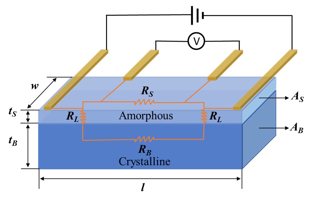
Four-probe contact measurement and corresponding lumped element model of a Ga-FIB device with an amorphous surface layer, with parallel bulk conducting channel
In the work by Cortie’s team, lateral patterns were etched on thin flakes of the materials using a focused ion beam (FIB) instrument at the University of Wollongong using gallium ions at low energy (5-30 keV) at varying fluences. The gallium ions penetrate only several nanometres into the material.
The researchers were able to combine ion beams and various forms of lithography to achieve dimensions smaller than 20 nanometres.
The ion irradiation, which was carried out with three types of interfaces under varying temperatures changed the atomic structure and the electronic properties.
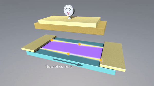
Importantly, the change in surface conductivity occurred at room temperature, suggesting a radical change in the electronic structure. To show this, key conducting atomic force microscopy measurements were performed by Dr Peggy Zhang, who is a Women-in-FLEET Fellow at the UNSW.
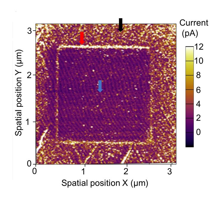
The current line scan profile shows high conductivity at the boundary between ion-beam irradiated and unirradiated areas
X-ray diffraction and cross-sectional transmission electron microscopy confirmed the phase transition and further experimentation with X-ray reflectometry and neutron reflectometry was used to gain insights into optimum ion beam dose to achieve the conversion.
Neutron reflectometry on the new Spatz instrument verified the thickness and morphology of the thin films and confirmed that the material remained the same chemical compound after the irradiation.
“The trick here is the judicious choice of the irradiation dose or what we normally call ion fluence. If you under-irradiate, very little happens to the structure, meanwhile, if you over- irradiate, you destroy the material via sputtering. We confirmed that we found the sweet spot for amorphisation,” said Dr Cortie.
The new X-ray reflectometer at the Australian Centre for Neutron Scattering confirmed the orientation and crystallisation of the Sb2Te3 below the nanometre-scale implanted region.
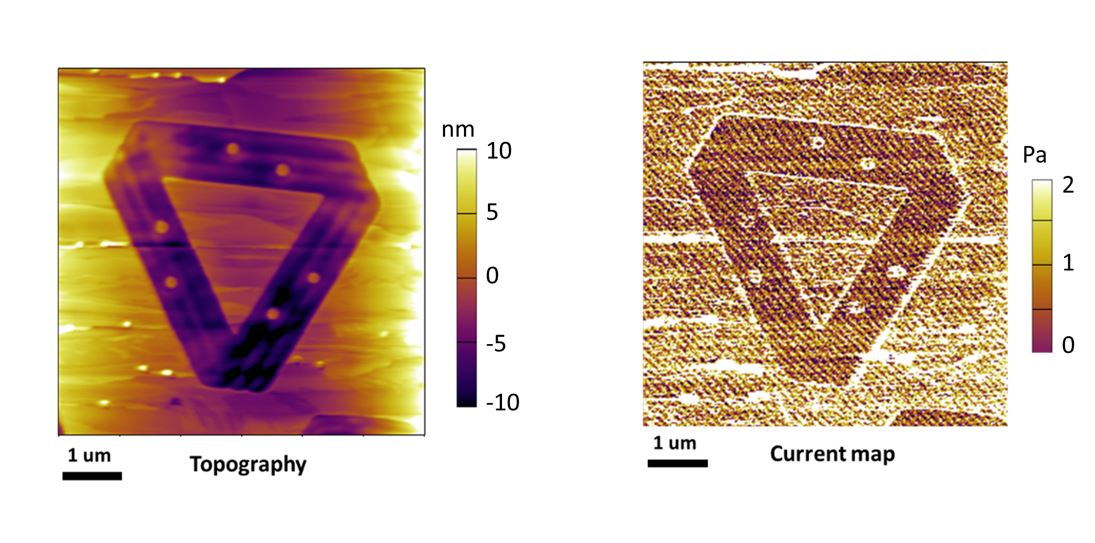
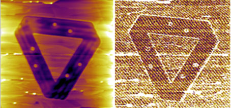
Using varying angles of the FLEET logo to demonstrate that edge effect on conductivity (with current mapped on RHS) is independent of scan direction wrt edge orientation
While early work made used of a focused ion beam instrument which is limited to very small sub-millimeter patterned regions, the researchers were later able to demonstrate the approach also worked on large wafer sized area cm2 sized films using a versatile low-energy (1-50 keV) ion implanter (LEII) on the Sirius accelerator at ANSTO’s Centre for Accelerator Science.
“Our implanter is optimised to implant ions in a relatively larger area than the focused ion beam instrument. We implant through a mask to a cover area from millimetres to centimetres,” explained Accelerator scientist Dr Zeljko Pastuovic.
Several different types of material were irradiated, including the antimony telluride, bismuth telluride and bismuth selenide.
Research Fellow Dr Peggy (Qi) Zhang (UNSW)
“Our system is very flexible, and can run many different types of ions, from light gases to metallic targets.”
The Centre for Accelerator Science supports research with ion implantation on electronic circuits for industrial and space applications.
Collaborating organisations included the University of Wollongong, FLEET, UNSW Sydney, RMIT, Technical University of Munich, University of Shanghai for Science and Technology, and Monash University.
The Australian Centre for Neutron Scattering has numerous collaborations in the semiconductor/quantum technology sectors, including leading international labs. ANSTO collaborates with Australian companies, such as Quantum Brilliance.
“The question of amorphous and quasicrystalline topological insulators is attracting a great deal of attention within the sector. Our work provides some of the first experiments and should be useful to many people working in this field,” said Dr Cortie.
“On the technological front, I also believe we have unveiled a very useful pathway towards scalable topological electronics utilising ion beams to define surface electronics”.
Top-down patterning of topological surface and edge states using a focused ion beam was published in Nature Communications in March 2023 (DOI 10.1038/s41467-023-37102-x)
more information
- Contact Dr David Cortie dcr@ansto.gov.au
- Visit ANSTO Centre for Accelerator Science