A UNSW study published last Friday presents an exciting step towards a novel form of electronics based on nano-scale, ‘disappearing’ conduction paths that could allow for extremely dense memory storage.
It’s based on domain walls, which are atomically sharp topological defects separating regions of uniform polarisation in ferroelectric materials.
The domain walls are electrically conductive, while the surrounding of the wall (ie, the bulk of the material) is insulating.
The relatively new discovery of domain-wall conductivity has given rise to a new technology: ‘domain wall nanoelectronics’, in which the wall (rather than the bulk of the material) stores binary data.
It’s a paradigm shift that hinges on nanoengineering of domain walls that can be precisely reconfigured by a controlling voltage.
Because domain walls are so small (only 1nm wide, or a millionth of a mm), topological effects cause structural changes that drastically alter the material’s properties. Essentially, you can think of the wall as being a completely different material to the surrounding material.
The electric dipoles in a domain wall can be influenced and reoriented by external electric fields (ie, by an applied voltage), so walls can be created, erased or relocated in the material. “This point is key to the new technology,” says researcher Nagy Valanoor. “It means that by manipulating a precisely-controlled voltage, we can create, erase or shift the conductive channels in which data is stored”.
It’s been called ‘agile’ circuitry.
Domain wall nanoelectronics could be a fraction of the size of traditional silicon (CMOS) technology. Domain walls 1 nm across compare favourably with CMOS structures that are typically 10 nm.
The most commonly studied form, magnetic domain walls, depend on the orientation of spin (intrinsic angular momentum) within domain walls. Magnetic domain walls have been investigated over the last decade for memory and logic applications.
Conversely, ferroelectric domain walls depend on the orientation of electric dipoles within the walls. Research in this field is more recent, but is seeing significant attention based on the potential for electronics that are ten to a hundred times smaller again than magnetic walls.
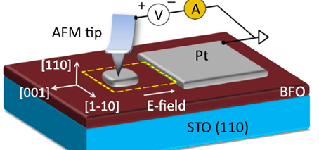
Using custom, nanofabricated electrodes and scanning probe techniques, the UNSW researchers demonstrated a novel ferroelectric domain wall memory that could be scaled down to less than 100 nm – excitingly close to CMOS scales for such an early, disruptive technology.
“Our new approach hinged on a way to stabilise nanoscale domain walls by using the right electrode geometry tailored to the properties of the specific materials we were using,” says UNSW researcher Jan Seidel. This was only possible by knowing the intricate material’s specific properties and a large amount of experience accumulated over 10+ years working in this area. “Our success came from high-quality material synthesis, years of experience of the team working with such materials, a highly beneficial work environment at UNSW and a good idea,” says Jan.
Information from the prototype device can be ‘read’ at moderate voltages with excellent endurance and retention characteristics, and has multilevel data storage capacity.
The work constitutes an important step toward integrated nanoscale ferroelectric domain wall memory devices.
Much of the work in ferromagnetic domain walls to date has been fundamental research, but proposals for commercialisation are being explored. “I think we are laying some of the groundwork at the moment for potential industrial uptake of our ideas and concepts,” says Jan Seidel.
The next steps are to show scalability of the memory concept to real device scales; to explore other, similar materials that would improve the memory performance and ideally to get more insight into the inner structure of such domain walls.
The study was published last week in Science Advances, the open-access journal published by the American Association for the Advancement of Science.
Lead author Pankaj Sharma and contributing authors Dan Sando, Jan Seidel and Nagarajan Valanoor are FLEET researchers at UNSW. Nanoelectronics, materials interfaces and topological structures are key to FLEET’s mission to develop new ultra-low energy electronics.
Funding support was provided by the Australian Research Council through Discovery Grants.
Want to learn more? You can follow FLEET on Twitter, watch a video on future solutions to computation energy use, or subscribe to FLEET news.