UNSW researchers solve a 10-year-old mystery in the way nanoscale transistors work.
Half of all the transistors in your iPhone use positively-charged ‘holes’, rather than negatively-charged electrons to operate.
At university, we teach undergraduates that holes are quasiparticles, basically ‘missing electrons’ – a bit like the bubble in a spirit level, or the missing chair in a game of musical chairs.
But that isn’t the whole story: holes also have very different ‘spin’ properties than electrons. (A particle’s spin is its intrinsic angular momentum.)
These unique spin properties of holes makes them very attractive for ultra-low powered spin transistors, high-speed quantum bits, and fault-tolerant topological quantum bits.
The problem is that until recently we didn’t have a good understanding of the spin properties of holes in nanoscale transistors. In fact, the best theories predicted the opposite behaviour to that observed in experiments.
Now, a team of physicists led by UNSW’s Alex Hamilton and Oleg Sushkov have solved the mystery by identifying a new term in the equations that had previously been overlooked.
This reconciles experiments and theory, and paves the way for future quantum electronic and quantum computing devices.
What they did
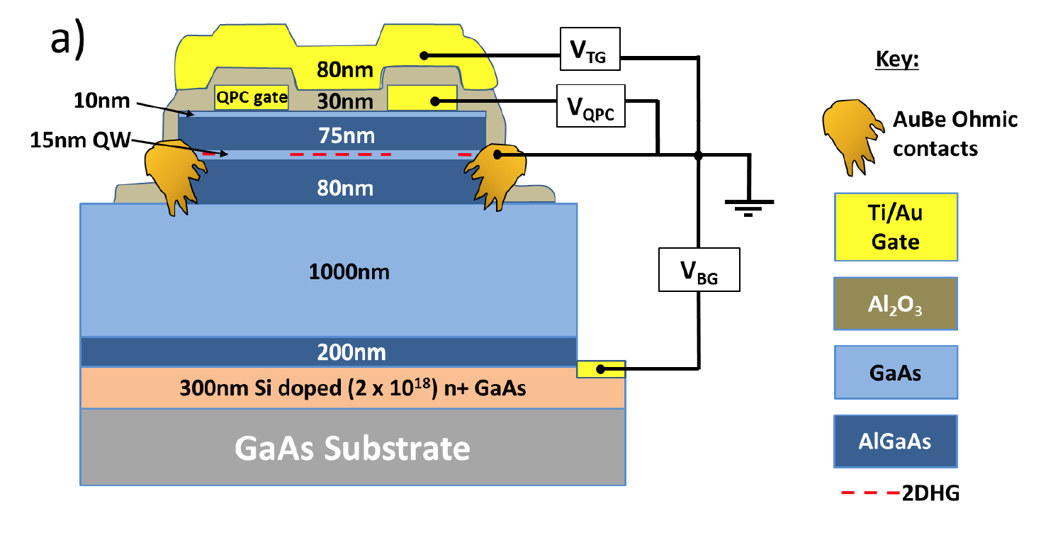
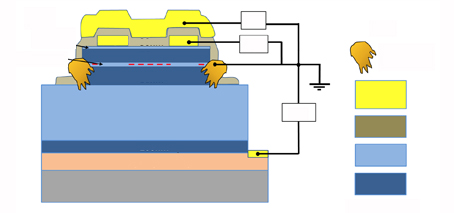
Schematic diagram of device showing how gate voltages are applied to control the electric field across the quantum wire
Key to the issue is that a hole behaves very differently when confined to only two-dimensions, compared with its behaviour in a normal, three-dimensional solid.
A transistor is manufactured with two semiconductor materials of slightly different electronic properties, pressed together. At the interface of those two materials, an effectively two-dimensional zone exists, in which a thin sheet of electrons or holes can be controlled to perform the necessary logical functions.
But while the behaviour of holes in three dimensions has been well understood for many decades, their confinement to two dimensions introduces new factors that cause otherwise-unpredictable responses to an applied magnetic field. Namely, this confinement introduces a new ‘spin–orbit interaction’.
Spin-orbit interaction (SOI), is the coupling of the hole’s movement through space (for example in orbit around an atom or along a current carrying path) and its spin. This spin-orbit interaction changes how holes respond to a magnetic field and is key to the function of topological materials, which are studied at FLEET for their potential to form ultra-low resistance pathways for electrical current.
The new study is the first time that these new spin-orbit effects for holes confined to one dimension have been properly classified.
Solving a ten-year mystery
In 2006, UNSW experiments found a result that did not match existing theory :
Experimenters were looking at the effects of an external magnetic field applied to a one-dimensional, charge-carrying path known as a quantum wire.
The applied magnetic field separates, or splits, the energy levels of holes with different spins. Experiments showed that the spin-splitting was extremely sensitive to the direction of the magnetic field, unlike electrons which are insensitive to the field direction.
Furthermore, the spin-splitting was found to be largest when the magnetic field was applied along the quantum wire – a result that was completely contrary to existing theories. This disagreement between experiment and theory remained unexplained for the past decade.
The most recent study identified a new spin-orbit interaction factor caused by the holes’ confinement to one dimension, and found that this new factor explained the 2006 experimental result.
The new study
The new study has just appeared in Physical Review Letters, the flagship journal of the American Physical Society.
The research joined theoretical and experimental physicists at UNSW with colleagues in Cambridge and Sheffield in the UK, and Novosibirsk in Russia.
The work was funded by the Australian Research Council Discovery Program, and included FLEET’s Alex Hamilton, Oleg Sushkov and Dima Miserev.
FLEET is a new, ARC-funded research centre aiming to address that growing computing energy challenge using materials that are just one atom in thickness. FLEET (the ARC Centre of Excellence in Future Low-Energy Electronics Technologies) is using atomically-thin, two dimensional (2D) materials as the basis of a new generation of ultra-low energy electronics. FLEET connects researchers from the UNSW School of Physics and the UNSW School of Materials Science and Engineering with colleagues in six other universities and 13 other Australian and international science centres.
Alex Hamilton leads FLEETs research theme 1, searching for topological dissipationless systems for future, ultra-low energy electronics.
The original 2006 research
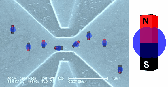
The alignment of holes with an applied magnetic field is shown in this animation
The original study in 2006, also led by Prof Hamilton and also published in Physical Review Letters, found that the direction of an applied magnetic field determined the splitting of conductivity in a current of holes. The same effect does not occur in a current of electrons.
This study was also the first to characterise the effect of a magnetic field on a current of holes along a quantum wire. The experiments showed that as holes travel along a one-dimensional path, their spins rotate to align with a magnetic field applied in a particular direction.
This response sets holes apart from electrons, which do not respond in the same way to changes – they don’t care which way the field is applied.
That unique property of holes gives exciting potential for their use in ‘spintronic’ technology. In spintronics, a particle’s magnetic spin is used to perform logical functions, rather than just the particle’s electrical charge, as in traditional electronics.
Some helpful definitions
Particle spin is an intrinsic angular momentum, and causes magnetism.
Two-dimensional materials are studied at FLEET for the potential to form ultra-low resistance paths down which current can flow. The most famous ‘2D’ material is graphene, a single sheet of carbon atoms. FLEET studies other 2D materials for their electronic properties. In the case of holes within a transistor, the 2D zone is formed not by the material itself, but by confinement of the charged particles to the interface between materials. Holes are confined at this interface by the voltage between the two semiconductors.
A quantum wire is a narrow constriction linking two hole/electron reservoirs, which are each confined to two-dimensions (ie, they exist in an infinitely flat plane). Because the channel is effectively one-dimensional, charged particles travelling long it experience quantum confinement perpendicular to their path. Effectively, travelling in ‘single file’. And thus the channel’s conductance (ie, how easily those charged particles flow along it) is quantised. Ie, the channel’s conductance increases in ‘step’ jumps.