
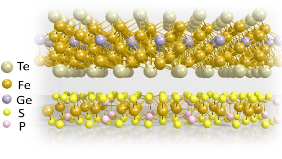
A heterostructure constructed with antiferromagnetic lower layer (FePS3) and ferromagnetic upper layer (Fe5GeTe2)
Electrical control of exchange bias effect in FePS3-Fe5GeTe2 van der Waals heterostructures via proton intercalations
A RMIT-led international collaboration published this week has observed, for the first time, electric gate-controlled exchange-bias effect in van der Waals (vdW) heterostructures, offering a promising platform for future energy-efficient, beyond-CMOS electronics.
The exchange-bias (EB) effect, which originates from interlayer magnetic coupling, has played a significant role in fundamental magnetics and spintronics since its discovery.
Although manipulating the EB effect by an electronic gate has been a significant goal in spintronics, until now, only very limited electrically-tunable EB effects have been demonstrated.
Electrical gate-manipulated EB effects in AFM-FM structures enable scalable energy-efficient spin-orbit logic, which is very promising for beyond-COMS devices in future low-energy electronic technologies.
The ‘blocking’ temperature of the EB effect can be effectively tuned via an electric gate, which would allow the EB field to be turned ‘ON’ and ‘OFF’ as well in future spintronic transistors.
The FLEET-led collaboration of researchers at RMIT University (Australia) and South China University of Technology (China) confirm for the first time the electric control of EB effect in a vdW heterostructure.
Realization of exchange bias effects in AFM-FM heterostructures

FLEET Research Fellow Dr Sultan Albarakati (RMIT)
The emergence of vdW magnetic materials boosts the development of vdW magnetic and spintronic devices and provides an ideal platform for exploring intrinsically interfacial magnetic coupling mechanisms.
Manipulating the EB effect, which originates from the AFM–FM interface coupling induced unidirectional anisotropy, by an electronic gate is a significant goal in spintronics. To date, very limited electrically tunable EB effects have been experimentally demonstrated in some oxide multiferroic thin film systems. Although vdW magnetic heterostructures have provided improved platforms to investigate EB effects, these heterostructures have not exhibited electrical gate-controlled EB effects yet.
“We had obtained much experience in vdW heterostructure-based nano-devices and we decided it was time for us to utilize some methods, such as electric gates, to control magnetic properties in FM/AFM bilayers,” says the study’s first author, FLEET Research Fellow Dr Sultan Albarakati (RMIT).
“Moreover, we are familiar with proton intercalation, which is an effective tool for modulating materials’ charge density.”
The team designed a nano-device structure with a tri-layer of FM/AFM/solid proton conductor, and chose a vdW material with higher Neel temperature, FePS3, to serve as the AFM layer.
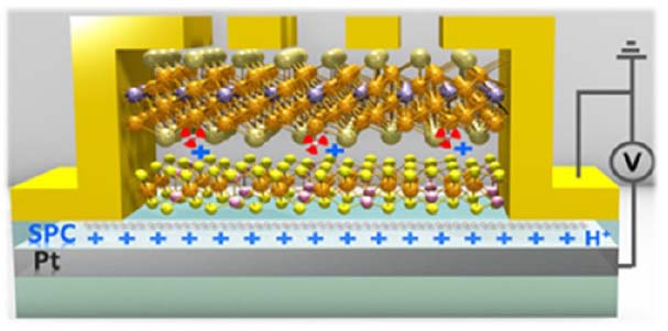
The device: a solid-proton field-effect transistor (SP-FET) mounts the AFM-FM heterostructure within electric contact (gold), mounted on a solid protonic conductor (SPC) and gate electrode (Pt)
“The choice of FM layer was a bit tricky,” says co-author Dr Cheng Tan (RMIT).
“Based on our previous results, the EB effect could occur in proton-intercalated Fe3GeTe2, while in Fe5GeTe2 (F5GT) of various thicknesses, the proton intercalation cannot result in any EB effects. Hence, we choose F5GT as the FM layer,” says Cheng.
Thus the resulting heterostructure comprised:
- Antiferromagnetic (AFM) layer FePS3 (FPS)
- Ferromagnetic (FM) layer Fe5GeTe2 (F5GT)
Generally, the EB effect is regarded as an interface effect and would be expected to diminish if the thickness of the FM layer is increased. While the thinner F5GT nano-flakes (<10 nm) can generate extremely large coercivity (Hc~2 T) due to the intralayer defect pinning, this make it more difficult to generate EB effect in a FM/AFM bilayer because the energy barrier induced by defect pinning is potentially larger than that from unidirectional anisotropy.
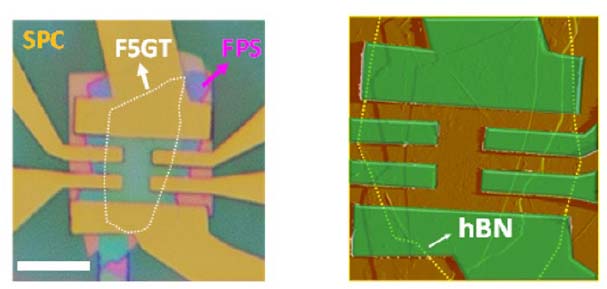
Imaging the device via optical microscope (left) and atomic force microscope (right)
“Our experimental observations are consistent with this,” explains co-author Dr Guolin Zheng (RMIT). “There is no occurrence of EB effects when the thickness of F5GT is less than 10 nm. Luckily, after many tests, we find that the EB effect can survive in FPS-F5GT heterointerfaces when the thickness of F5GT layer is within the range of 12 nm to 20 nm.”
“Then we could further explore the effects of proton intercalations in FPS-F5GT.” says Guolin.
Electrically-controlling the exchange bias effect via proton intercalation
The team then successfully performed the proton intercalation in FPS-F5GT and observed the shift of EB fields under different gate voltages.
FLEET Research Fellow Dr Guolin Zheng (RMIT)
“The blocking temperature of the EB effect can be effectively tuned via electric gate. And more interestingly, the EB field can be switched ‘ON’ and ‘OFF’ repeatably under various gate voltages,” says Guolin.
Further theoretical calculations carried out by collaborator from South China University of Technology further confirms that the proton intercalations not only tune the average magnetic exchange coupling but also change the antiferromagnetic configurations in the FePS3 layer.
“The gate-dependent EB effects can be well-explained based on our calculations,” says contributing-author A/Prof Lan Wang (also at RMIT). “Under different proton intercalations, the affected AFM-FM coupling-induced unidirectional anisotropy energy and the transformation of FPS3 between an uncompensated AFM and a compensated AFM lead to the various interesting phenomena.”
“Again, this study is a significant step towards vdW heterostructure-based magnetic logic for future low-energy electronics.”
The study
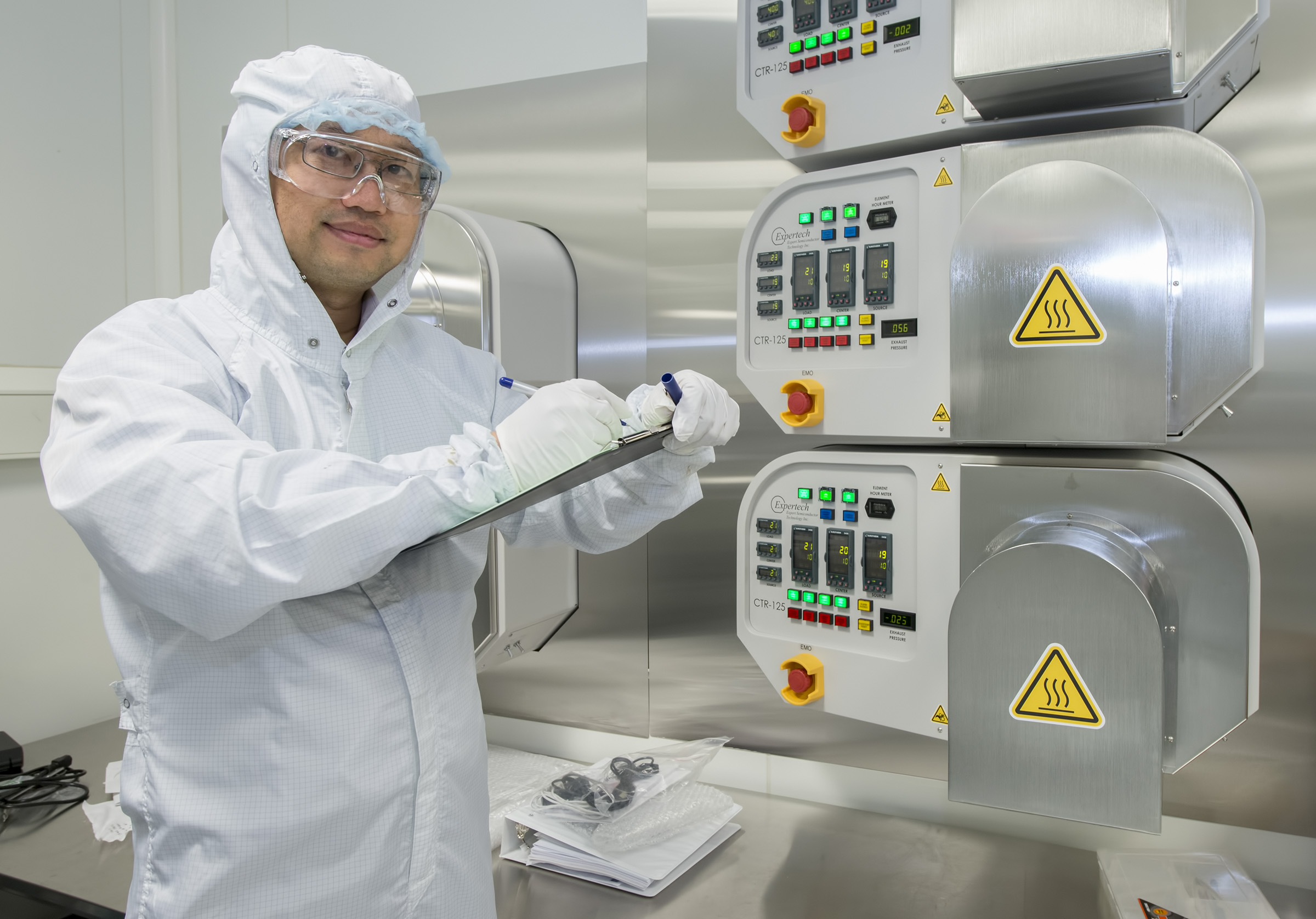
A/Prof Lan Wang in Class 100 clean room,
RMIT
“Electric Control of Exchange Bias Effect in FePS3−Fe5GeTe2 van der Waals Heterostructures” was published in Nano Letters in August 2022. (DOI: 10.1021/acs.nanolett.2c01370)
As well as support from the Australian Research Council, support was also provided by Natural Science Foundation of China, the National Key Research and Development Program of China, the Fundamental Research Funds for the Central Universities, the Collaborative Innovation Program of Hefei Science Center and the High Magnetic Field Laboratory (China).
Experimental research was performed at the RMIT Micro Nano Research Facility (MNRF) in the Victorian Node of the Australian National Fabrication Facility (ANFF) and the RMIT Microscopy and Microanalysis Facility (RMMF).
Spintronics are studied within FLEET’s enabling technology B — nano-device fabrication. The Australian Research Council Centre of Excellence in Future Low-Energy Electronics Technologies (FLEET) brings together over a hundred Australian and international experts, with the shared mission to develop a new generation of ultra-low energy electronics. The impetus behind such work is the increasing challenge of energy used in computation, which uses 5–8% of global electricity and is doubling every decade.
More information
- Contact Dr Sultan Albarakati (RMIT) sultan.albarakati@rmit.edu.au
- Contact Dr Guolin Zheng (RMIT) glzheng@rmit.edu.au
- Contact A/Prof Lan Wang (RMIT) lan.wang@rmit.edu.au
- Watch Future solutions to computation energy use
- Connect @FLEETCentre