
Why 2D? What is it about two-dimensional materials that makes them so interesting for FLEET?
FLEET UNSW/Wollongong collaboration finds transition point from 3D to 2D properties
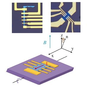
2D WTe2 samples (upper) and experimental schematic (lower) diagram of angle-dependent measurement configuration.
Constraining the movement of charge carriers (electrons or holes) to two dimensions unlocks unusual quantum properties, resulting in useful electronic properties.
Although we refer to the layers within such materials as ‘2D’, they are not strictly two dimensional. What’s key is the restriction of a particle’s movement perpendicular to the plane of the material a scale that is proportional to the de Broglie wavelength of the particle.
In essence, this means the range from a few hundred nanometres down to a few nanometres.
Much can be learned by observing precisely at what thickness such new effects emerge.
A FLEET study published last week in Physical Review B quantifies the precise transition point in the promising material tungsten ditelluride (WTe2).
Measurements found:
- WTe2 thin films cross from 3D to 2D electronic systems at thickness of ~ 20 nm
- overlap between conduction and valence bands decrease at thickness below ~12 nm, implying that even thinner samples might achieve a bandgap.
FLEET Research Fellow Feixiang Xiang (right) studies electron transport through topological edge states in 2D WTe2 crystals
The study began under FLEET CI Xiaolin Wang at the University of Wollongong, with FLEET Research Fellow Dr Feixiang Xiang first studying the special electronic structure of bulk WTe2 samples that leads to the material’s very large magnetoresistance (previously published).
Feixiang then prepared thin films of different thickness cleaved from a single crystal using micro-exfoliation onto a substrate.
After study of WTe2 thin films at UOW, Feixiang used UNSW laboratories to fabricate the devices from thin-film samples and perform transport measurements using ultralow temperature and high magnetic field measurement facilities.
Alignment markers, electrodes, and bonding pads were fabricated by E-beam lithography.
Angle-dependent quantum oscillation measurements were performed in very high magnetic fields at FLEET CI Alex Hamilton’s lab at UNSW, revealing how the material’s band structure changed with decreasing thickness, with a 3D–2D crossover when the sample thickness was reduced below 26 nm.
“This finding was very important,” says Feixiang Xiang, who led the study at both UOW and UNSW, “because it pins down two critical length scales of the thickness-dependent electronic structure in WTe2 thin films.”
Analysis indicated that the area of Fermi pockets decreases in thinner samples, suggesting the overlap between the conduction band and valence band becoming smaller. This not only explains the measured decrease of carrier density in a thinner sample, it suggests it is possible to open a band gap and realize the 2D topological insulator in even thin samples, as has been predicted by theory, and observed in related compounds (MoS2 and MoTe2).
Tungsten ditelluride (WTe2) is a layered, transition metal dichalcogenide with several promising properties:
- extremely large magnetoresistance, with potential for use in magnetic sensors
- bulk WTe2 predicted to be a type-II Weyl semimetal
- monolayer WTe2 is a high temperature topological insulator, a superconductor, and a ferroelectric.
Transition metal dichalcogenides (TMDs) are a class of van der Waals materials, comprising many atomically-thin atomic layers bound by weak intermolecular forces.
We refer to TMDs as ‘2D’ because of this layered crystal structure.
Constraining the movement of charge carriers to two dimensions results in very different electronic properties compared to 3D ‘bulk’ materials, which also suggests that more, different physical properties could happen at the monolayer limit – the transition point from 3D to 2D.
The study Thickness dependent electronic structure in WTe2 thin films was published in the American Physical Society’s journal Physical Review B in July 2018.
Acknowledgement Research was in part funded by the Australian Research Council under the Discovery Project and Future Fellowship funds and FLEET’s Centre of Excellence funding, the Guangdong Innovative and Entrepreneurial Research Team Program and the Science, Technology, and Innovation Commission of Shenzhen Municipality, and was performed in part using facilities of the NSW and ACT Nodes of the Australian National Fabrication Facility.
Study of novel materials and topological insulators at FLEET
![]() The electronic properties of WTe2 and other TMDs are studied at FLEET, which is an Australian Research Council Centre of Excellence.
The electronic properties of WTe2 and other TMDs are studied at FLEET, which is an Australian Research Council Centre of Excellence.
The Centre for Future Low-Energy Electronics Technologies (FLEET) brings together over a hundred Australian and international experts, with the shared mission to develop a new generation of ultra-low energy electronics.
Study co-author Prof Alex Hamilton heads FLEET’s study of topological materials, which aims to produce an ultra-low energy topological transistor. Prof Xiaolin Wang (UOW and ISEM) leads FLEET’s atomically thin and novel materials technology research.
The impetus behind such work is the increasing challenge of energy used in computation, which uses 5–8% of global electricity and is doubling every decade.
More information
- Study contact Dr Feixiang Xiang feixiang.xiang@unsw.edu.au
- UNSW Prof Alex Hamilton Alex.Hamilton@unsw.edu.au
- UOW/ISEM Prof Xiaolin Wang xiaolin@uow.edu.au
- FLEET media@FLEET.org.au
- Visit FLEET.org.au
- Follow @FLEETCentre
- Watch Future solutions to computation energy use
- Subscribe FLEET.org.au/news