- Significant step toward future topological electronics
- The first electric field-switchable topological material
- Topological transistors would be an ultra-low energy , beyond CMOS solution to ICT energy use after the end of Moore’s Law
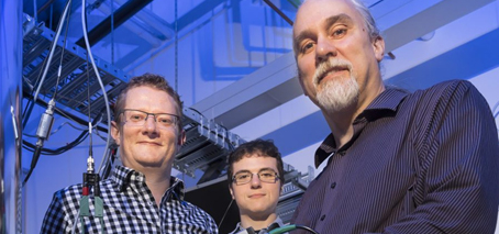
Study authors (from left) Dr Mark Edmonds, James Collins and Prof Michael Fuhrer are in the School of Physics and Astronomy at Monash University.
Over the last decade, there has been much excitement about the discovery, recognised by the Nobel Prize in Physics only two years ago, that there are two types of insulators: normal insulators which don’t conduct electricity, and topological insulators – newly discovered materials that conduct electricity only on their edges.
Now, FLEET researchers at Monash University, Australia, have for the first time successfully ‘switched’ a material between these two states of matter via application of an electric-field. This is the first step in creating a functioning topological transistor – a proposed new generation of ultra-low energy electronic devices.
Ultra-low energy electronics such as topological transistors would allow computing to continue to grow, without being limited by available energy as we near the end of achievable improvements in traditional, silicon-based electronics (a phenomenon known as the end of Moore’s Law).
“Ultra-low energy topological electronics are a potential answer to the increasing challenge of energy wasted in modern computing,” explains study author Professor Michael Fuhrer.
“Information and Communications Technology (ICT) already consumes 8% of global electricity, and that’s doubling every decade.”
This new study is a major advance towards that goal of a functioning topological transistor.
How it works: Topological materials and topological transistors
Topological insulators are novel materials that behave as electrical insulators in their interior, but can carry a current along their edges.
“In these edge paths, electrons can only travel in one direction,” explains lead author Dr Mark Edmonds. “And this means there can be no ‘back-scattering,’ which is what causes electrical resistance in conventional electrical conductors.”
Unlike conventional electrical conductors, such topological edge paths can carry electrical current with near-zero dissipation of energy, meaning that topological transistors could burn much less energy than conventional electronics. They could also potentially switch must faster.
Topological materials would form a transistor’s active, ‘channel’ component, accomplishing the binary operation used in computing, switching between open (0) and closed (1).
“This new switch works on a fundamentally different principle than the transistors in today’s computers,” explains Dr Edmonds. “We envision such switches facilitating a completely new computing technology, which uses lower energy.”
The electric field induces a quantum transition from ‘topological’ insulator to conventional insulator.
To be a viable alternative to current, silicon-based technology (CMOS), topological transistors must:
- operate at room temperature (without the need for expensive supercooling),
- ‘switch’ between conducting (1) and non-conducting (0), and
- switch extremely rapidly, by application of an electric field.”
While switchable topological insulators have been proposed in theory, this is the first time that experiment has proved that a material can switch at room temperature, which is crucial for any viable replacement technology.
(In this study, experiments were conducted at cryogenic temperatures, but the large band-gap measured confirms that the material will switch properly at room temperatures.)
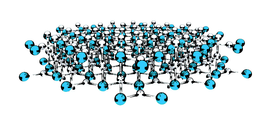
Na3Bi structure shown with sodium atoms white and bismuth atoms blue
The material Na3Bi is a topological Dirac semimetal (TDS), which have long been considered promising systems in which to look for topological field-effect switching, as they lie at the boundary between conventional and topological phases.
The study found that when Na3Bi is made ‘atomically thin’ (ie, only a few layers of atoms in thickness), it is possible to open an electronic band gap, turning the material into an insulator. This bandgap is an essential component in any electronic switch.
ICT energy use, the end of Moore’s Law and ‘Beyond CMOS’ solutions
The overarching challenge behind the work is the growing amount of energy used in information and communication technology (ICT), a large component of which is driven by switching.
Each time a transistor switches, a tiny amount of energy is burnt, and with trillions of transistors switching billions of times per second, this energy adds up.
The power-efficiency of CMOS electronics is plateauing
For many years, the energy demands of an exponentially growing number of computations was kept in check by ever-more efficient, and ever-more compact CMOS (silicon based) microchips – an effect related to the famous ‘Moore’s Law’. But as fundamental physics limits are approached, Moore’s Law is ending, and there are limited future efficiencies to be found.
“The information technology revolution has improved our lives, and we want it to continue,” says Prof Michael Fuhrer.
“But for computation to continue to grow, to keep up with changing demands, we need more-efficient electronics.”
“We need a new type of transistor that burns less energy when it switches.”
“This discovery is a step in the direction of topological transistors that could transform the world of computation.”
- The energy burnt in computation accounts for 8% of global electricity use
- ICT energy use is doubling every decade
- ICT contributes as much to climate change as the aviation industry
- Moore’s Law, which has kept ICT energy in check for 50 years, will end in the next decade.
The study
FLEET researchers used scanning probe microscopy/spectroscopy (STM/STS) and angle-resolved photoelectron spectroscopy (ARPES) to study the structure and electronic state of Na3Bi.
The study Electric Field-Tuned Topological Phase Transition in Ultra-Thin Na3Bi was published today in Nature. (DOI 10.1038/s41586-018-0788-5)
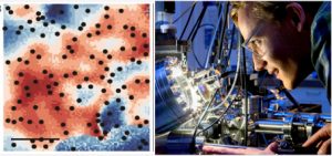
Study author James Collins, Advanced Light Source, California
Facilities Na3Bi crystal growth and STM measurement was conducted in FLEET’s laboratories at Monash University, and at the Advanced Light Source (Lawrence Berkeley National Laboratory), in California, where ARPES measurements were made. Research was also undertaken on the soft X-ray beamline at the Australian Synchrotron.
Acknowledgements The study was funded by the Australian Research Council’s Centres of Excellence and DECRA Fellowship programs, while travel to Berkeley was funded by the Australian Synchrotron.
Results
The researchers found that:
- In the absence of an electrical field, atomically-thin Na3Bi is a 2D topological insulator with a ‘bulk’ (ie, interior) bandgap >300 meV (ie, behaving as an electrical insulator), and no bandgap at the edges (ie only the edges conduct electricity, and they conduct without dissipation).
- At a critical applied electrical field, the bandgap closes to zero everywhere, and the material becomes a semimetal like graphene (ie, it conducts everywhere – interior and edges).
- Above that critical electrical field, the bandgap opens everywhere (to 90meV) and there is no conduction (interior and edges).
“These large bandgaps are much greater than the thermal energy available at room temperature (25meV),” explains study author James Collins. “Which demonstrates that ultrathin Na3Bi is suitable for room-temperature topological transistor operation.”
“Ie, the material is capable of dissipationless transport of charge at room temperature.”
Topological materials and FLEET
Topological materials are investigated within FLEET’s Research theme 1, seeking ultra-low resistance electronic paths with which to create a new generation of ultra-low energy electronics.
FLEET is an Australian Research Council-funded research centre bringing together over a hundred Australian and international experts to develop a new generation of ultra-low energy electronics, motivated by the need to reduce the energy consumed by computing.
More information
- Contact Dr Mark Edmonds, School of Physics and Astronomy, Monash University mark.edmonds@monash.edu
- Connect at @FLEETCentre
- Visit FLEET.org.au
- Read FLEET Research theme 1 news
- Contact FLEET media@FLEET.org.au
- Watch Future solutions to computation energy use
- Subscribe FLEET.org.au/news
Images
All images are available at high-resolution and permission is given to publish elsewhere in connection with this story.
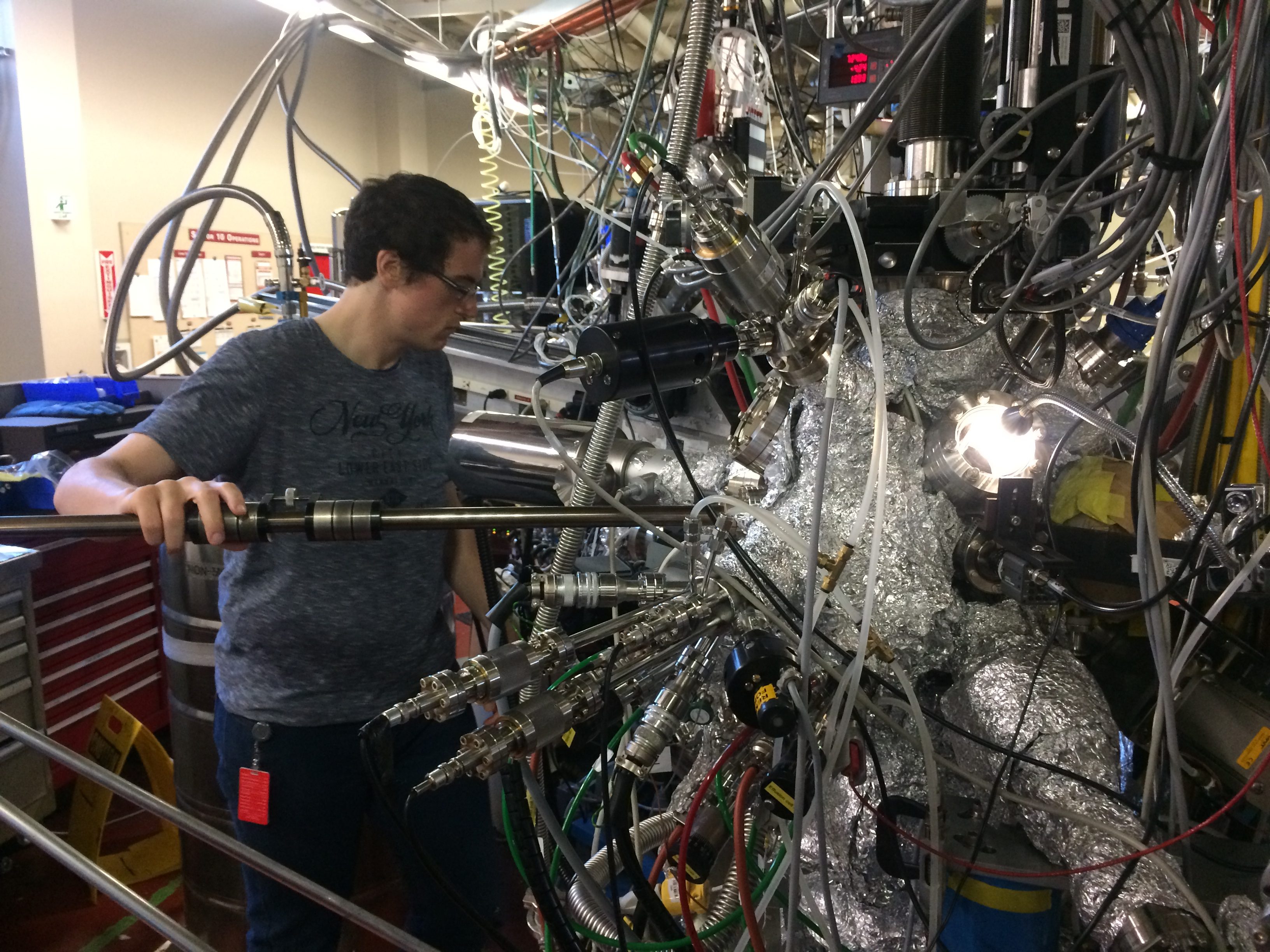
James Collins
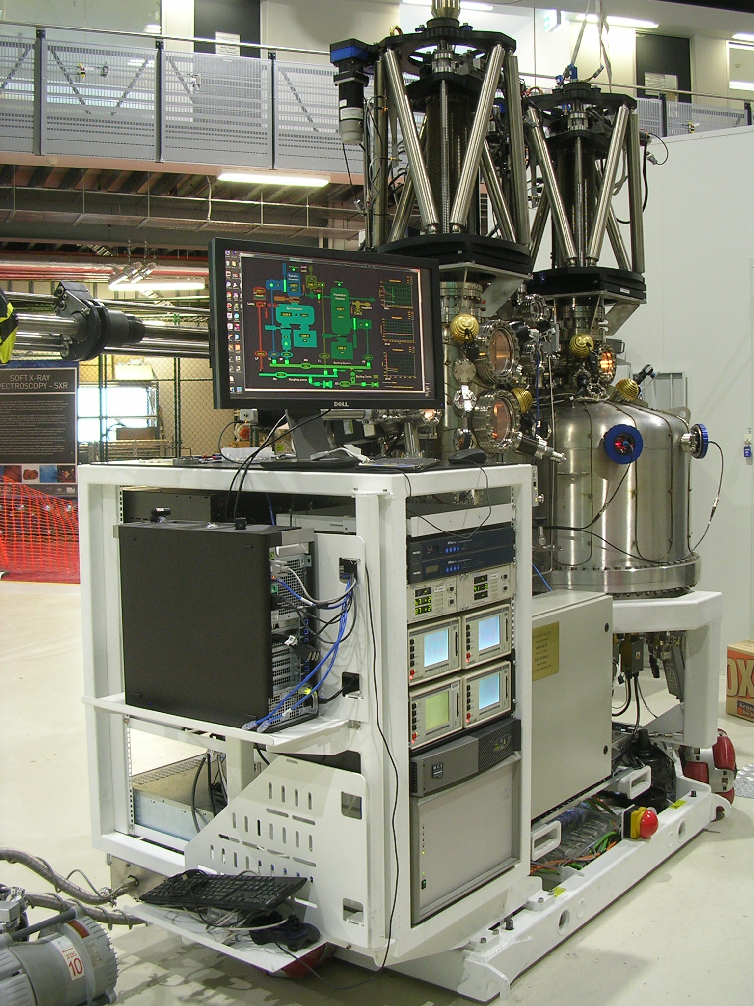
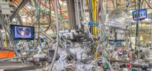
New ARPES facility at the Australian Synchrotron
Study author James Collins, Advanced Light Source, California
FLEET Director Professor Michael Fuhrer at the Centre Launch, 12 June
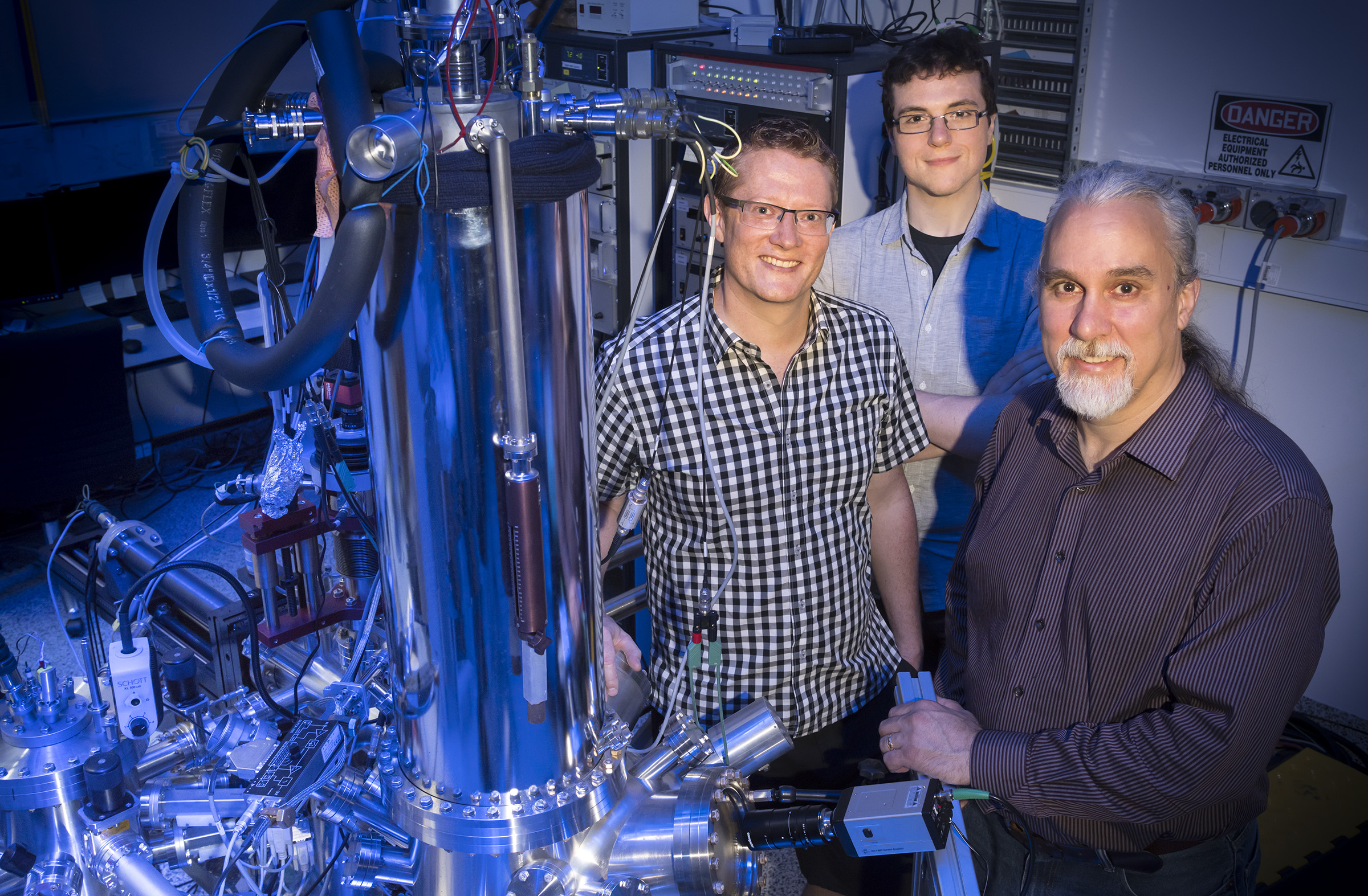
Mark Edmonds, James Collins and Michael Fuhrer in the labs at Monash University
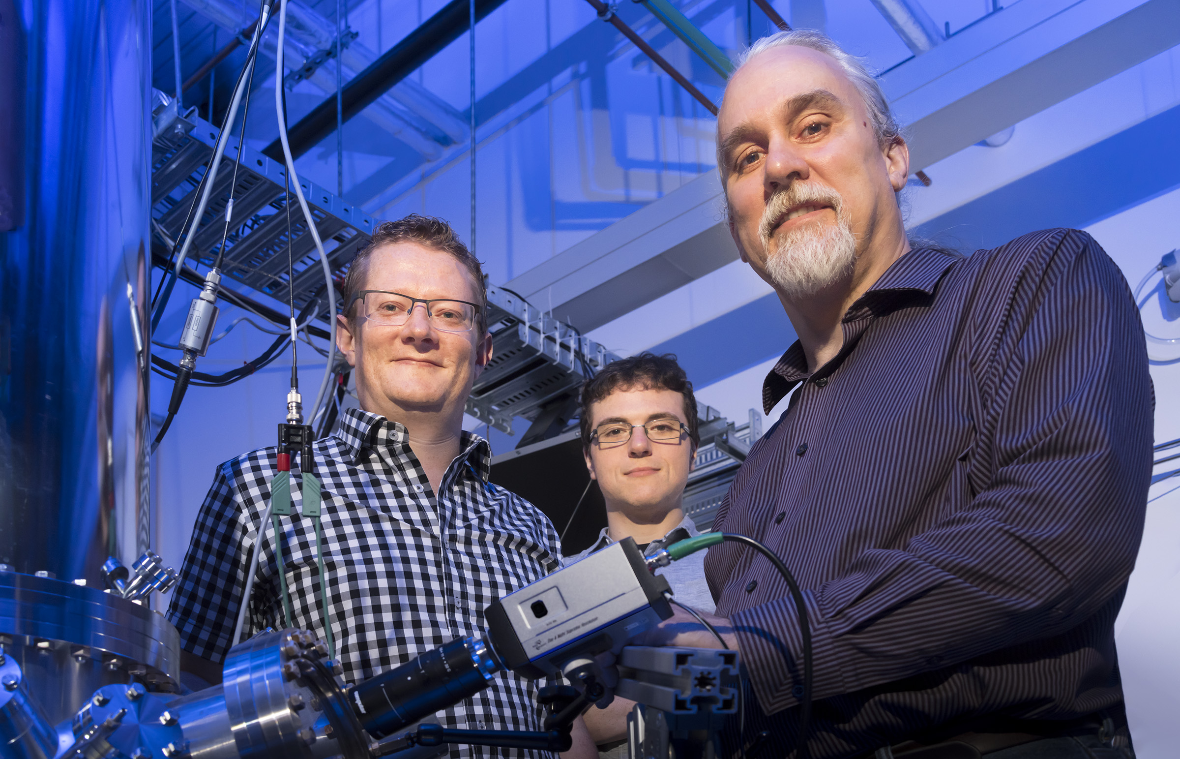
Study authors (from left) Dr Mark Edmonds, James Collins and Prof Michael Fuhrer are in the School of Physics and Astronomy at Monash University.
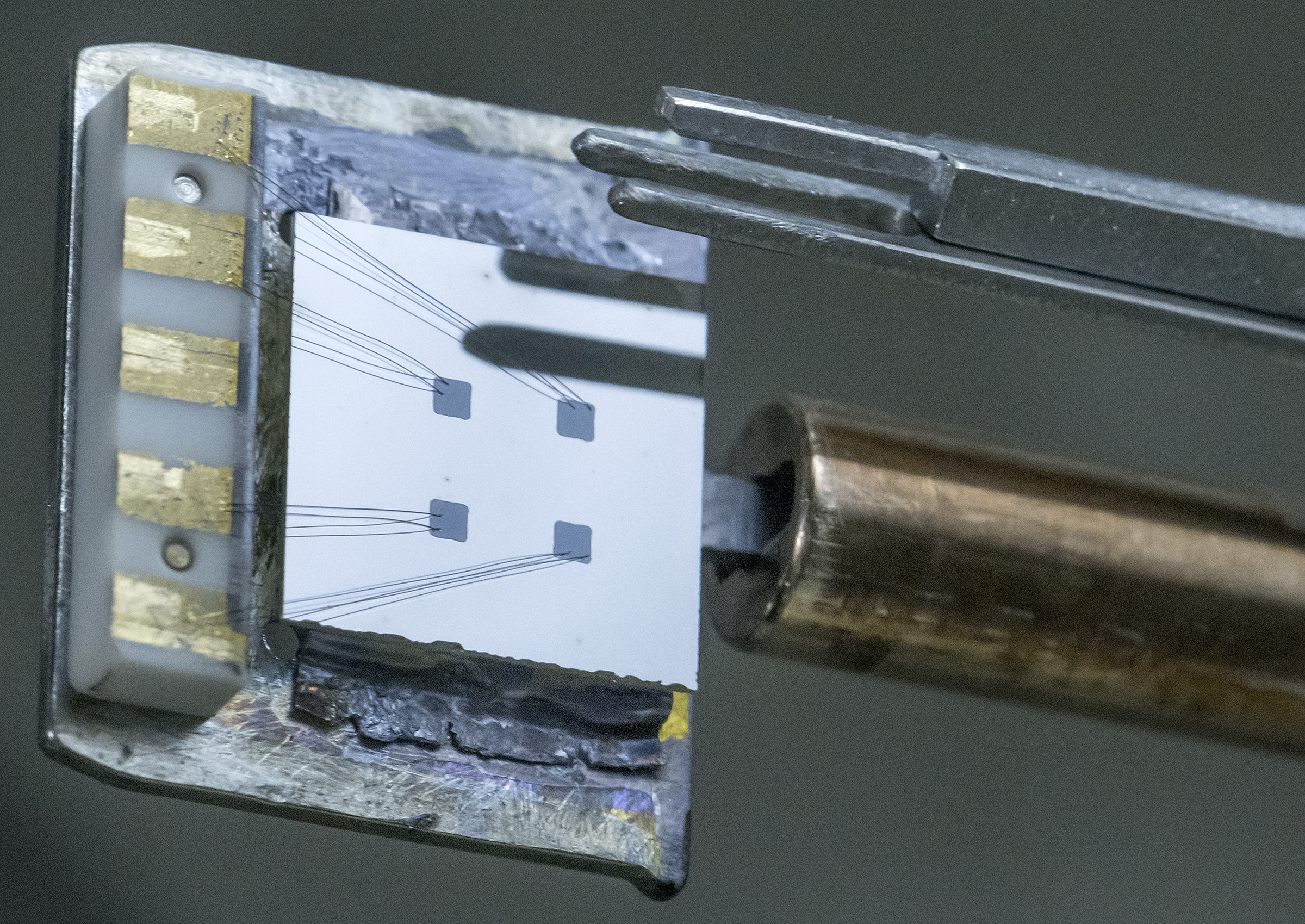
Thin film of Na3Bi grown on sapphire with gold contacts to allow for electrical measurements of the carrier density and mobility at low temperature in a magnetic field
Previous stories
Explainer: zeroes and ones and the transistors at the heart of computing

Explainer: glossary of terms
The case for FLEET: 8% of global electricity now consumed by computing
Switching conduction mode: a step towards topological transistors
Studying electronic structure on Berkeley beamlines
Electronically-smooth ‘3d graphene’: a bright future for Na3Bi
Collaborating FLEET personnel:
- Associate Investigator Mark Edmonds (Monash University)
- Partner Investigator Anton Tadich (Australian Synchrotron)
- PhD student Chang Liu (Monash University)
- PhD student James Collins (Monash University)
- Associate Investigator Shaffique Adam (Yale-NUS)
- Director and CI Michael Fuhrer (Monash University)