- Spin-gapless semiconductors (SGSs) are a new class of zero-gap materials, with fully spin polarized electrons and holes.
- SGSs bridge the zero-gap materials and half-metals
- Material’s fascinating spin and charge states hold great potential for future spintronic technology.
A University of Wollongong team has published an extensive review of spin-gapless semiconductors (SGSs) .
Spin gapless semiconductors (SGSs) are a new class of zero gap materials which have fully spin polarised electrons and holes.
The study tightens the search for materials that would allow for ultra-fast, ultra-low energy ‘spintronic‘ electronics with no wasted dissipation of energy from electrical conduction.
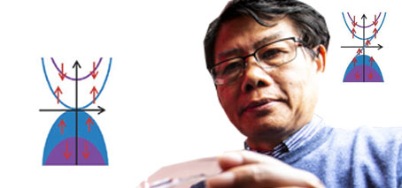
Their defining property of SGS materials relates to their ‘bandgap’, the gap between the material’s valence and conduction bands, which defines their electronic properties.
In general, one spin channel (ie, one of the spin directions, up or down) is semiconducting with a finite band gap, while the other spin channel has a closed (zero) band gap.
In a spin-gapless semiconductor (SGS), conduction and valence band edges touch in one spin channel, and no threshold energy is required to move electrons from occupied (valence) states to empty (conduction) states.
This property gives these materials unique properties: their band structures are extremely sensitive to external influences (eg, pressure or magnetic field).
Most of the SGS materials are all ferromagnetic materials with high Curie temperatures.
The band structures of the SGSs can have two types of energy–momentum dispersions: Dirac (linear) dispersion or parabolic dispersion.
The new review investigates both Dirac and the three sub-types of parabolic SGSs in different material systems.
For Dirac type SGS, their electron mobility is two to four orders of magnitude higher than in classical semiconductors. Very little energy is needed to excite electrons in an SGS, charge concentrations are very easily ‘tuneable’. For example, this can be done by introducing a new element (doping) or by application of a magnetic or electric field (gating).
The Dirac type spin gapless semiconductors exhibit fully spin polarized Dirac cones and offer a platform for spintronics and low-energy consumption electronics via dissipationless edge states driven by the quantum anomalous Hall effect.
“Potential applications of SGSs in next-generation spintronic devices are outlined, along with low- electronics, and optoelectronics with high speed and low energy consumption.” according to Professor Xiaolin Wang, who is the Director of Institute for Superconducting and Electronic Materials, UoW and the theme leader of FLEET.
Since spin-gapless semiconductors (SGSs) were first proposed by s Professor Xiaolin Wang in 2008, efforts worldwide to find suitable candidate materials have particularly focussed on Dirac type SGSs.

The band structures of parabolic and Dirac type SGS materials with spin-orbital coupling, which leads to the quantum anomalous Hall effect.
In the past decade, a large number of Dirac or parabolic type SGSs have been predicted by density functional theory, and some parabolic SGSs have been experimentally demonstrated in both monolayer and bulk materials.
The review
The review paper Spin-Gapless Semiconductors was published in the journal Small in June 2020 (DOI 10.1002/smll.201905155).
The authors acknowledge funding support from the Australian Research Council through the Centre of Excellence program, and thank Tania Silver for her contribution.
Bandgap physics: an explainer
In solid-state band theory, materials in nature can be classified as metals, insulators or semiconductors based on their electronic band structures.
A valence band contains a material’s highest energy electrons. Just ‘above’ this (ie, more energetic) is the conduction band, which is the lowest band of vacant electronic states.
In a metal, conduction electrons located in the conduction band, so that electrons (ie, an electric current) can flow easily in a metal. In an insulator, the two bands are separated by a large gap so that electrons cannot flow. In semiconductors, such as the silicon that forms the basis of traditional integrated circuits and transistors, the bands are separated by a smaller gap, so that the application of a small threshold energy can boost electrons into the conduction band. This is essentially how silicon transistors ‘switch’.
Novel materials at FLEET
 The properties of novel and atomically-thin materials are studied at FLEET, an Australian Research Council Centre of Excellence, within the Centre’s Enabling technology A.
The Centre for Future Low-Energy Electronics Technologies (FLEET) is a collaboration of over a hundred researchers, seeking to develop ultra-low energy electronics to face the challenge of energy use in computation, which already consumes 8% of global electricity, and is doubling each decade.
Review co-author Prof Xiaolin Wang leads FLEET’s University of Wollongong node, as well as leading the Enabling Technology team developing the novel and atomically thin materials underpinning FLEET’s search for ultra-low energy electronics, managing synthesis and characterisation of novel 2D materials at the University of Wollongong
Prof Wang leads FLEET’s efforts to exploit charge and spin quantum effects in magnetic topological insulators as well as fabricating high-quality samples for joint research with FLEET researchers at Monash, UNSW, ANU and RMIT.
Dr Zengji Yue is a FLEET Research Fellow working alongside Prof Wang at the Institute for Superconducting & Electronic Materials and Australian Institute for Innovative Materials (AIIM) in University of Wollongong, Australia. Dr Yue’s research focuses on nanofabrication, quantum transport, and optics of topological and spin gapless materials. He designs and fabricates electronic and optical devices taking advantage of novel physics of topological materials.
More information
- Contact author Dr Zengji Yue zengji@uow.edu.au
- Contact author Prof Xiaolin Wang xiaolin@uow.edu.au
- Follow @FLEETCentre