FLEET’s mission to create ultra-low energy electronics depends on an improved fundamental understanding of the electronic structure of atomically-thin, two-dimensional materials.
We need to understand how electrons in the material interact with each other and also how they move and scatter through the crystal lattice.
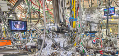
FLEET researchers using the vacuum ultraviolet the UV beamline 10.0.1 (HERS) at the Advanced Light Source (Lawrence Berkeley National Laboratory, in California) last month took advantage of the facility’s unique arrangement of material-growth and measurement techniques to investigate candidate materials for large-bandgap topological insulators.
The Berkeley beamline combines a molecular beam epitaxy (MBE) crystal growth facility ‘in line’ with an electronic-structure measurement technique known as ARPES.
The in-line setup allows researchers to grow atomically-thin materials and measure their properties both during and after the growth process, all within the same sealed vacuum chamber, so that the material remains in pristine condition.
Synchrotron light sources such as the ALS provide a number of spectroscopic and imaging techniques, designed to investigate the atomic arrangement and electronic structure of materials.
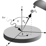
In ARPES, synchrotron radiation causes electron emission from the subject material. Energy and momentum of outgoing electrons reveal the fundamental behaviour of electrons within the material (its electronic bandstructure).
Angle Resolved Photoelectron Spectroscopy (ARPES) is a particular synchrotron measurement technique that measures the behaviour of electrons moving through the crystal lattice, which determines the material’s fundamental electronic properties.
Using ARPES, researchers study electrons emitted from the material as it is bombarded with synchrotron radiation. ARPES measures both the energy and direction (momentum) of the outgoing electrons, which reveals important details of the electronic structure.
Based at Berkely for most of July, Monash University’s Mark Edmonds and the Australian Synchrotron’s Anton Tadich used the MBE growth chamber and ARPES analysis at beamline 10.0.1 to grow and study candidate materials.
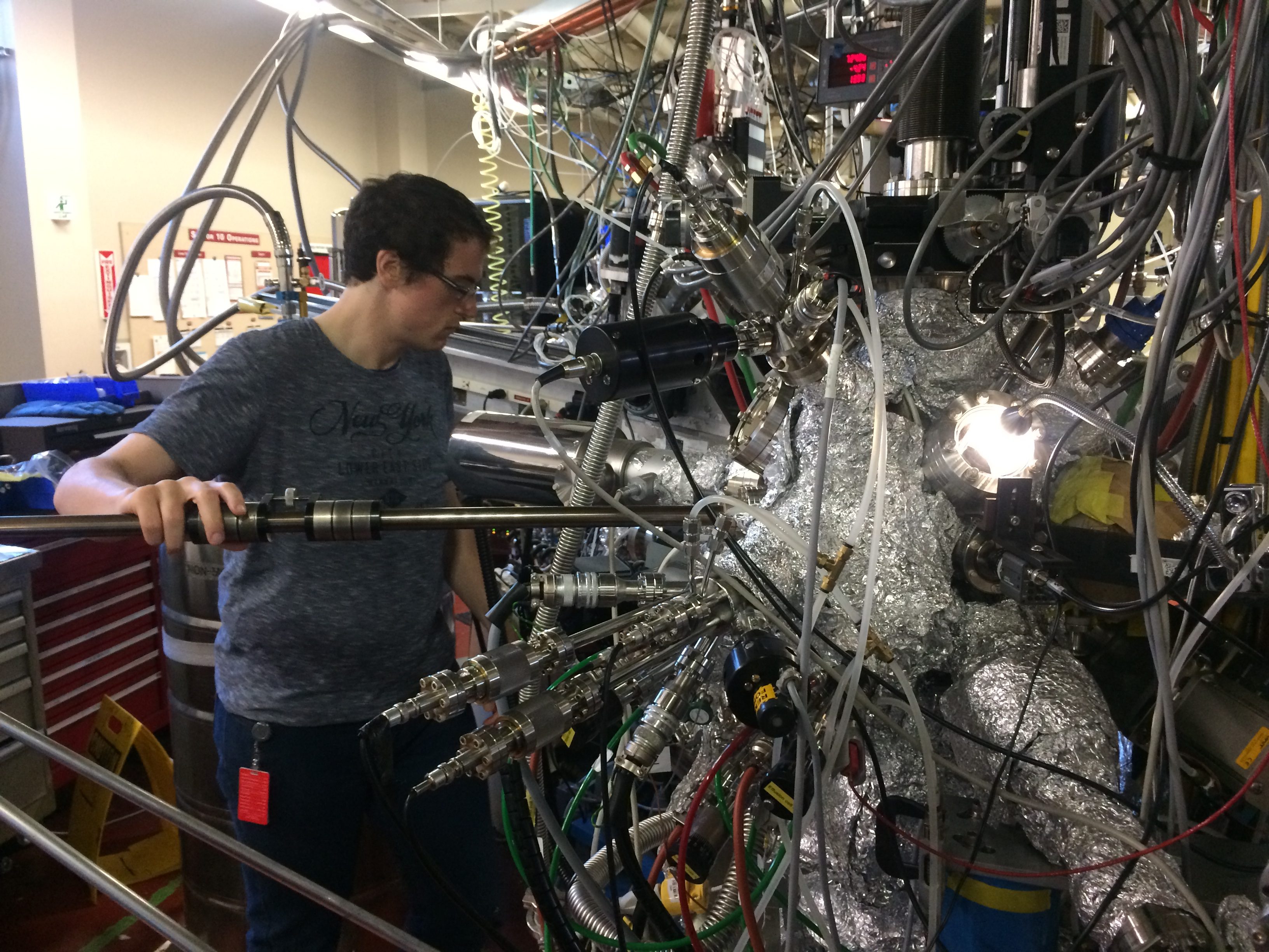
James Collins (Monash University) setting up equipment at ALS
ARPES is the most ‘direct’ method we have to determine electronic structure of these materials,” says Anton. “The technique lets us excite electrons using synchrotron light to drive them outside of the material, and we can then infer how they were originally behaving inside the material.”
From the resulting data, researchers determine the fundamental behaviour of the electrons within the material – the ‘electronic band-structure’, which determines whether it will function as a topological insulator.
A larger bandgap means the material will be a topological insulator at higher temperatures,” says Mark Edmonds. “We’re looking for materials that will still be topological at room temperature, and thus retain the dissipationless edge paths that are key to developing functional low-energy electronics.”
Work to date has found many materials that operate as topological insulators at very low temperatures. However if a data centre needed to be cooled to a few degrees Kelvin to operate, any energy gains in the electronics would be vastly outweighed by the energy needed to cool the facility.
The research was funded by an ARC DECRA grant, Monash Centre for Atomically Thin Materials and the Australian Synchrotron’s International Synchrotron Access Program.
Mark Edmonds (ARC DECRA Fellow, Monash University) specialises in thin-film grow of topological materials, and characterising those materials with ARPES and Scanning Tunneling Microscopy (STM), and is working on realising large-gap topological insulators in two dimensions in FLEET’s Research Theme 1.
Anton Tadich (beamline scientist at Australian Synchrotron) specialises in photoemission from novel materials, and is a partner investigator within FLEET. Anton will manage ARPES measurements on a new toroidal analyser to be installed on the Australian Synchrotron’s soft X-ray beamline.

The new toroidal analyser at Australian Synchrotron, Oct 2017
The toroidal analyser to be installed at the Synchrotron later this year will allow complementary in situ growth and characterisation of topological materials via ARPES (electronic properties) and Scanning Tunneling Spectroscopy (STM), a powerful probe for measuring atomic-level structure and localised electronic properties. The Australian Synchrotron is a FLEET Partner Organisation.
Want to learn more? You can follow FLEET on Twitter, watch a video on future solutions to computation energy use, or subscribe to FLEET news.